
The Untold Stories of IoT Device Teardowns and Hardware Reverse Engineering
28 min read Explore behind-the-scenes insights from IoT device teardowns, revealing hidden components, debug ports, firmware pitfalls, and security lessons, with real-world examples, toolkits, and ethical guidelines for responsible hardware reverse engineering. (0 Reviews)
You’ve probably seen the glossy marketing photos of a sleek smart speaker, a trim wearable, or an elegant thermostat that promises efficiency, safety, and a dash of magic. But behind the glass and polymer is a tightly negotiated ecosystem of silicon decisions, supply chain pivots, power compromises, and security trade-offs—most of which never make it to the spec sheet. IoT device teardowns and hardware reverse engineering pull back the veil, not to glorify destruction, but to understand how things are really built, where they succeed, and why they sometimes fail. These are the untold stories that shape what ends up in our homes and factories—and what we can learn to build better next time.
What a Teardown Really Reveals

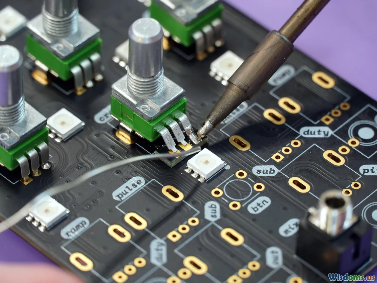
A responsible teardown isn’t about prying for the sake of it; it’s an inquiry into the decisions that turn requirements into reality. Open a smart plug—or ethically, review credible teardown photos—and you’ll often see an AC-DC power stage with a compact flyback converter, a microcontroller module (ESP32 or RTL8710-class in many budget devices), a relay with physical separation from low-voltage logic, and antennas snaked into tight corners to save space. These images tell a story:
- Component choice: Are passives mostly 0603 or 0402? Smaller parts fit tighter spaces but complicate rework and may heat differently under load. High-volume consumer devices often use 0402 to shave millimeters and cost.
- Power priorities: Look for heat sinks, thermal vias, and copper pours around switching regulators. The presence of an NTC inrush limiter or a MOV surge protector hints at consideration for line spikes and longevity.
- Materials and safety: Flame-retardant plastics (UL 94 V-0) in power-adjacent areas, adequate creepage and clearance between high and low voltage, and conformal coating for moisture protection tell you the product was built for real-world messiness.
- Modular strategy: Off-the-shelf wireless modules reduce certification overhead (FCC/CE) and help teams ship faster. Spotting a canned RF module suggests a trade-off between design control and time-to-market.
These details, in aggregate, reveal how a device manages cost, compliance, and performance—and whether it respects the very real constraints of life outside a product roadmap slide.
Reading the Bill of Materials Like a Detective

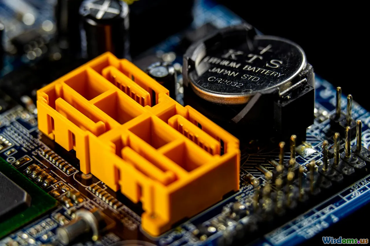
In most teardowns, the BOM is the Rosetta Stone. The large IC with a laser-etched code and a logo might be easy to identify, but the real insight comes from the supporting cast. A smart sensor cluster that pairs a Nordic nRF52-series SoC with a discrete power amplifier and an external flash is telling you something: BLE range mattered, and the firmware image or data logging was non-trivial. A surprising FRAM chip might indicate frequent write cycles—perhaps for metering or event logs where endurance matters.
Real-world cases show how BOMs reflect supply-chain pressures:
- The 2020–2022 chip shortages pushed many teams to second-source regulators and MEMS sensors. Teardowns from that period often show footprint-compatible alternates designed into the PCB from day one, a quiet hedge against delays.
- In cost-constrained consumer gadgets, it’s common to see a single switcher feeding multiple rails with LDOs doing fine trimming. Industrial gear, by contrast, often opts for separate, robust rails to reduce interference and improve diagnostics.
- For IoT cameras, teardowns sometimes reveal image sensors paired with beefy DRAM to buffer frames before compression. The DRAM brand and die size can foreshadow performance under low light or high-motion scenes.
Look beyond the headline chip: the specific oscillator stability, EMI filter topology, and even connector choice (board-to-board vs. FFC) speak volumes about what the product team feared most—noise, shock, or assembly yield.
The Moments Designs Meet Reality: Failure Modes in the Wild

Teardowns often document failure modes that no simulation fully predicted. A few recurring lessons:
- Thermal ghosts: Smart lights pack drivers, Wi-Fi, and LED strings into confined spaces. We’ve seen discolored PCBs where LED resistors act as localized heaters. Over many cycles, FR-4 darkening can correlate with increasing drive current and color shift, or premature LED failures.
- Mechanical fatigue: Button assemblies on wearables frequently fail where a steel dome meets a flexible PCB. Even quality domes succumb if adhesives creep or the housing tolerances drift.
- Moisture migration: Conformal coatings (acrylic or silicone) are common in industrial IoT. Consumer devices often skip them to save cost, leading to corrosion around battery terminals in humid climates. The telltale sign is verdigris on copper pads and intermittent behavior long before total failure.
- Power spikes: Budget smart plugs occasionally show inadequate creepage between mains and logic. Some teardowns have flagged gaps under 2 mm where 3–6 mm is more typical for durable designs, depending on standards and conditions. Even if a unit passes initial tests, long-term arcs and carbon tracking can spell danger.
Failure analysis isn’t finger-pointing; it’s pattern recognition. It shows where assumptions about users, environment, or lifecycle collided with reality and suggests how future revisions can survive the messy middle of product life.
Security Without Scaring Your Customers: What Debug Ports Teach Us
Open hardware isn’t the same as insecure hardware, and debug interfaces aren’t villains. Yet many teardowns find unprotected debug ports or unlock mechanisms that rely on obscurity. Responsible research highlights both the good and the risky—without giving a blueprint to misuse.
What often emerges:
- Mature products burn fuses to disable unrestricted debug or implement authenticated debug protocols. Security-first products pair secure boot with signed firmware updates and encrypted storage.
- Cost-driven devices sometimes leave UART or SWD test pads accessible after mass production, with minimal restrictions. Engineers often meant to remove or lock these for final units but ran out of time.
- Adding epoxy over a key IC sounds defensive but can interfere with heat dissipation and rework while offering limited real protection. Better approaches include silicon with hardware root of trust, key storage in secure elements, and formal vulnerability disclosure processes.
A healthy teardown culture frames these findings as shared learning: celebrate designs that implement defense in depth; encourage routine red-teaming; and remind stakeholders that legality and user safety are non-negotiable. If a teardown reveals a risky pattern, a coordinated disclosure (aligned with standards like ISO/IEC 29147 and 30111) helps vendors fix issues without stoking panic.
How to Read a Teardown Photo Set Like a Pro

You don’t need a lab to learn from teardowns. A disciplined way to review photos can level-up your product sense without handling tools or hardware.
- Power path mapping: Trace from the input connector to switching components, inductors, and regulators. Note heat sinks, big caps, and keep-out zones. Ask: Where does heat go? What happens during surges?
- RF hints: Identify antenna placement and ground clearance. A meandering trace or ceramic chip antenna near metal housing could limit range. Shield cans often hide RF front ends—observe their location relative to noise sources like DC-DC converters.
- Assembly and serviceability: Spot fasteners vs. adhesive seams. Excessive glue on connectors may stabilize during drop tests but complicate repair and recycling. Look for standardized connectors in industrial designs versus custom flex in consumer gear.
- Sensors and isolation: In mains-connected devices with low-voltage sensing, watch for opto-isolators or differential amplifiers indicating thoughtful separation. Lack of isolation in unexpected places is a flag for deeper review.
Treat each photo as a tiny audit: what does it say about priorities, and what questions does it raise about long-term reliability?
The Economics Behind the Screws: Cost, Certification, and Compromises

A teardown can’t perfectly predict margins, but it reveals cost gravity. Consider a $30 smart plug:
- BOM gravity: AC-DC conversion (transformer, switcher IC, protection) can consume a surprising slice of cost. Add a relay rated at 10–16 A with proper spacing, then a Wi-Fi/BLE module, and the numbers climb before plastic tooling or packaging.
- NRE and certification: FCC/CE, safety (UL/IEC), and radio approvals cost time and money. Many brands adopt pre-certified wireless modules to compress timelines—something you can spot in teardowns.
- Manufacturing yield: Choices like 0402 passives and tight flex harnesses save space but can depress yields and raise test costs. You might notice test pads placed to enable automated fixtures—an indirect signal that the team anticipated yield challenges.
- Firmware overhead: External flash or FRAM, extra RAM, or a microcontroller variant with crypto accelerators points to complex software. Complexity correlates with development time and post-launch maintenance obligations.
Teardowns show how companies convert market price constraints into design discipline—or sometimes, unfortunate shortcuts.
Industrial vs. Consumer IoT: A Tale of Two Philosophies

Place a consumer smart sensor next to an industrial one, and the differences are almost tactile:
- Enclosures: Industrial gear boasts IP65–IP67 ratings, robust seals, and UV-stable plastics; consumer shells prioritize aesthetics and weight. Splash-resistant designs turn into dust- and solvent-resistant units with the right gasketing and screws—but at cost.
- Connectors: M12 and aviation-style connectors with locking rings dominate in factories; consumer devices use USB-C or pogo pins. In teardowns, ruggedized connectors often have strain relief and are over-specified for lifecycle.
- Coatings and range: Industrial PCBs frequently feature conformal coatings and wider copper pours for thermal mass. You may see RS-485, CAN, or 4–20 mA interfaces instead of Wi-Fi, designed for noisy environments.
- Temperature budgets: -40 to +85 °C for industrial vs. 0 to +40 °C for many consumer devices. That drives component selection: quartz oscillators with better stability, derated capacitors, and larger inductors.
Comparisons in teardowns crystallize the idea that “more robust” isn’t a vibe; it’s a pile of specific decisions about materials, connectors, and derating.
Safety, Legality, and Ethics: Practicing Responsible Curiosity
Curiosity is a force for good when paired with care. If you’re engaging with hardware analysis in any form, a few responsible practices help keep people and data safe:
- Safety first: Lithium cells can vent violently if punctured or mishandled. Mains voltages can be lethal. Treat power systems with respect. Follow ESD precautions to avoid device damage.
- Legal boundaries: Reverse engineering laws vary. Always work on hardware you own or have explicit permission to analyze, and never attempt to bypass security or access data you’re not authorized to handle.
- Coordinated disclosure: If a concerning pattern emerges from a teardown (e.g., potential safety hazard or security weakness), contact the manufacturer and follow recognized disclosure practices. Publicly shaming products before giving teams a chance to fix rarely improves outcomes.
- Respect user trust: Teardown journalism and research should avoid exposing personally identifying information or providing exploitable specifics that could enable unauthorized access.
Done right, teardown culture educates without enabling harm and nudges the entire industry toward safer defaults.
What Designers Can Learn from the “Inside Story”
Teardowns let designers benchmark against the state of the art without guesswork. Key takeaways that surface repeatedly:
- Put heat where it can leave: Thermal vias under power ICs, copper pours that spread load, and components with clear airflow paths correlate strongly with reliability.
- Design for second sources: Footprint-compatible regulators and sensors can mitigate shortages. PCB footprints with flexible pinouts offer future-proofing when the supply chain bites back.
- Use defense in depth: Secure boot, signed updates, and minimized attack surfaces work in concert. Teardowns often highlight how piecemeal security (e.g., epoxy blobs) underperforms systemic controls.
- Plan for service and recycling: Over-glued assemblies and exotic fasteners frustrate repair, inflate e-waste, and can alienate savvy customers. Fasteners and modular sub-assemblies are an investment in brand goodwill and sustainability.
- Test with reality in mind: Environmental stress screening and HALT/HASS aren’t luxuries for industrial only. Consumer teardowns reveal where vibration, sweat, or kitchen grease defeated clever but fragile constructions.
There’s a reason many teams keep a “tear down wall” in the lab. Seeing different solutions to the same constraints builds intuition, faster than any spec sheet can.
Environmental Stakes and the Right-to-Repair Momentum

The practical outcomes of teardown culture tie directly to sustainability. According to the UN’s Global E-waste Monitor 2024, the world generated roughly 62 million metric tons of e-waste in 2022—much of it difficult to recycle due to adhesives, mixed materials, and tightly integrated assemblies. Thoughtful design reduces this burden:
- Fasteners over adhesives: Screws and clips allow part separation for repair and recycling. Adhesives can be strategic for sealing, but blanket use traps materials together.
- Standard cells and ports: Replaceable batteries and common connectors keep devices in service longer. Soldered or proprietary approaches can strand otherwise functional hardware.
- Transparency pays off: Public teardowns pressure brands to justify design choices that impede serviceability. It’s not just a moral stance; it’s reputational capital and, increasingly, regulatory compliance in some markets.
Right-to-repair laws and ecodesign initiatives in the EU and several US states are aligning incentives. When the inside story is visible, it’s harder to favor disposable architectures over maintainable ones.
Case Files: Surprises Teardowns Keep Turning Up

Every year brings a few memorable finds:
- The budget smart plug with an overly optimistic relay: A device advertised for space heaters used a relay barely adequate for steady-state current, with minimal thermal relief on the PCB. Under repeated switching, discoloration around the contacts suggested rising resistance and heat—an avoidable risk with better derating.
- The wearable with epoxy armor: An activity tracker used black epoxy to cover both the SoC and PMIC. A teardown found hotspots aligning with those packages and measured thermal throttling during longer sessions. Later revisions swapped materials and added copper slugs under the packages, markedly improving comfort and battery life.
- The “surprise” secure update: A late-model smart display looked ordinary inside—until investigators noted a secure element paired with its application processor. Public materials had never trumpeted secure boot, but teardown clues and test behavior suggested signed updates and encrypted storage were in place. Quiet good news is still good news.
- The modular gateway that saved a recall: An industrial gateway had a radio module with a known field issue. Because the module was socketed and the enclosure accessible, the vendor shipped replacements and instructions for authorized service partners. A potentially devastating recall became a manageable module swap.
These stories reinforce that the inside of a product is a constantly iterated negotiation. Sometimes the wins are invisible; sometimes the misses are instructive.
Practical, Non-Destructive Ways Teams Use Teardown Insights

You don’t have to open competitors’ products to learn from the practice. Organizations leverage teardown thinking in safe, constructive ways:
- Design reviews with external exemplars: Keep a curated library of public teardown photos. Use them to benchmark layout density, thermal strategies, and shielding approaches during your own design reviews.
- Material choices backed by evidence: Tie enclosure and gasket decisions to examples from products in similar conditions. For instance, conformal coating use in outdoor sensors has an extensive visual record.
- Lifecycle modeling: Observe where others place test pads and strain relief, then adapt your own test strategy accordingly. Teardowns reveal how mature companies build for manufacturing diagnostics.
- Procurement leverage: Recognize commodity vs. specialty parts in the wild. If every device in your category has migrated to a certain PMIC, you gain negotiating power—or know when to avoid supply bottlenecks.
This “teardown mindset” turns external observation into internal discipline without crossing ethical or legal lines.
Choosing Tools Without Going Overboard

In the public imagination, reverse engineering labs brim with exotic gear. In reality, most insights come from careful observation and documentation, sometimes aided by common tools:
- Optics: A modest digital microscope reveals solder quality, component markings, and stress indicators. You don’t need micron-level metrology to learn from a board’s story.
- Measurement: Basic multimeters and non-contact thermometers can validate heat paths and power rails indirectly. Engineers often triangulate with thermal cameras for rapid iteration.
- X-ray and CT: Advanced labs use X-ray imaging to inspect solder joints under BGAs or verify internal routing. It’s invaluable for quality assurance and failure analysis.
Even with tools, responsible practice avoids exposing secrets that could enable misuse. The goal is understanding the why and the trade-offs—not cracking locks.
Design Patterns Worth Emulating from the Best Teardowns

Patterns that appear in well-resolved designs, across categories:
- Clear isolation: Obvious safety separation between high- and low-voltage domains; routed slots under opto-isolators; careful alignment of shield cans far from noisy power stages.
- Thermal choreography: Heat-generating components are not clustered; copper pours make sense; thermal interfaces are honest about the enclosure’s ability to sink heat.
- Service-friendly bits: Connectors that click, not glue; batteries that unclip, not pry; mechanicals designed to survive a second assembly without shattering.
- Test foresight: Well-placed test points, intentional ground access, and fiducials for pick-and-place reliability. It’s the sign of a team that expected to learn during ramp, not just hope.
- Security that scales: Secure boot and update paths that persist across chip revisions and product families. In strong examples, the chain of trust is productized, not custom each time.
Spotting these strategies helps teams avoid reinvention and consumers recognize quality beyond the spec sheet.
The Bigger Picture: Standards, Interoperability, and the Road Ahead

Looking forward, several currents will shape what future teardowns reveal:
- Interoperability pressures: Initiatives like Matter are nudging vendors toward predictable network behavior. Expect more standardized radio subsystems and consistent secure commissioning flows.
- Security hardening: More MCUs are shipping with secure enclaves, hardware root of trust, and authenticated debug. Physical debug access is shrinking as on-die features mature.
- SIM goes silicon: iSIM and eSIM reduce the footprint and tamper surfaces for cellular IoT, consolidating previously separate components and tightening the update story.
- Chip supply pragmatism: After recent shortages, designs are baking in alternates and modularity at the PCB and firmware layers to hedge risk, visible through footprint flexibility and pin-compatible families.
- Sustainability by design: Regulatory and consumer pressure favor maintainable products. Expect to see more screws, fewer destructive adhesives, and clearer battery replacement paths.
- Edge AI footprint: As MCUs with ML accelerators proliferate, teardowns will reveal paired memory and optimized power rails necessary for bursty inference workloads.
The inside story will keep evolving, but the theme is consistent: less mystique, more engineering honesty.
A final thought: the magic of a great IoT product isn’t diminished by understanding it; it’s amplified. When a teardown shows careful thermal paths, thoughtful isolation, real security, and materials that age gracefully, it reads like a love letter to good engineering. And when it exposes rushed shortcuts, that too is a service—an invitation to do better, and a reminder that what we embed in the physical world deserves our best habits. The next time you press a smart button or glance at a sensor’s tiny LED, remember: there’s a quiet drama under that shell. Learning from it is how we build the next generation with fewer regrets and more resilience.
Rate the Post
User Reviews
Other posts in Reverse Engineering


Popular Posts